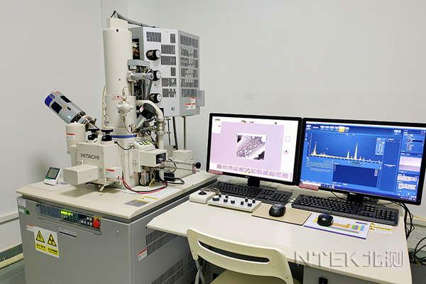
The scanning electron microscope (SEM) is an observation technique between the transmission electron microscope and the optical microscope. It can directly observe nanomaterials, perform fracture surface analysis and observe original surfaces. A focused, very narrow high-energy electron beam scans the sample; the interaction between the beam and matter excites various physical signals, which are collected, amplified and imaged to characterise the microscopic morphology of the material. Modern SEM resolution reaches 1 nm, magnification reaches 300,000x and above with continuous adjustment, and depth of field and field of view are large with good three-dimensional imaging. Combined with other analytical instruments, SEM can also perform micro-area composition analysis while observing morphology. SEM is widely used in the study of rock and soil, graphite, ceramics and nanomaterials, and therefore plays a major role in scientific research.









 WeChat Official Account
 Submit successfully